Intel displays tech to build extreme multi-chiplet packages 12 times the size of the largest AI processors, beating TSMC's biggest — floorplan the size of a cellphone, armed with HBM5, 14A compute tiles and 18A SRAM
Big things can only get bigger.

Get 3DTested's best news and in-depth reviews, straight to your inbox.
You are now subscribed
Your newsletter sign-up was successful
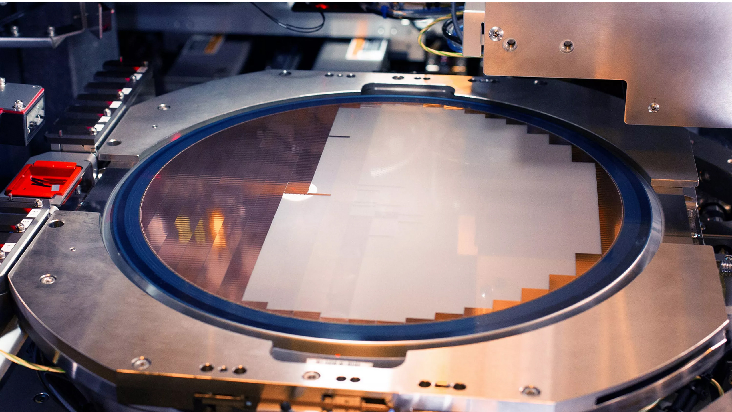
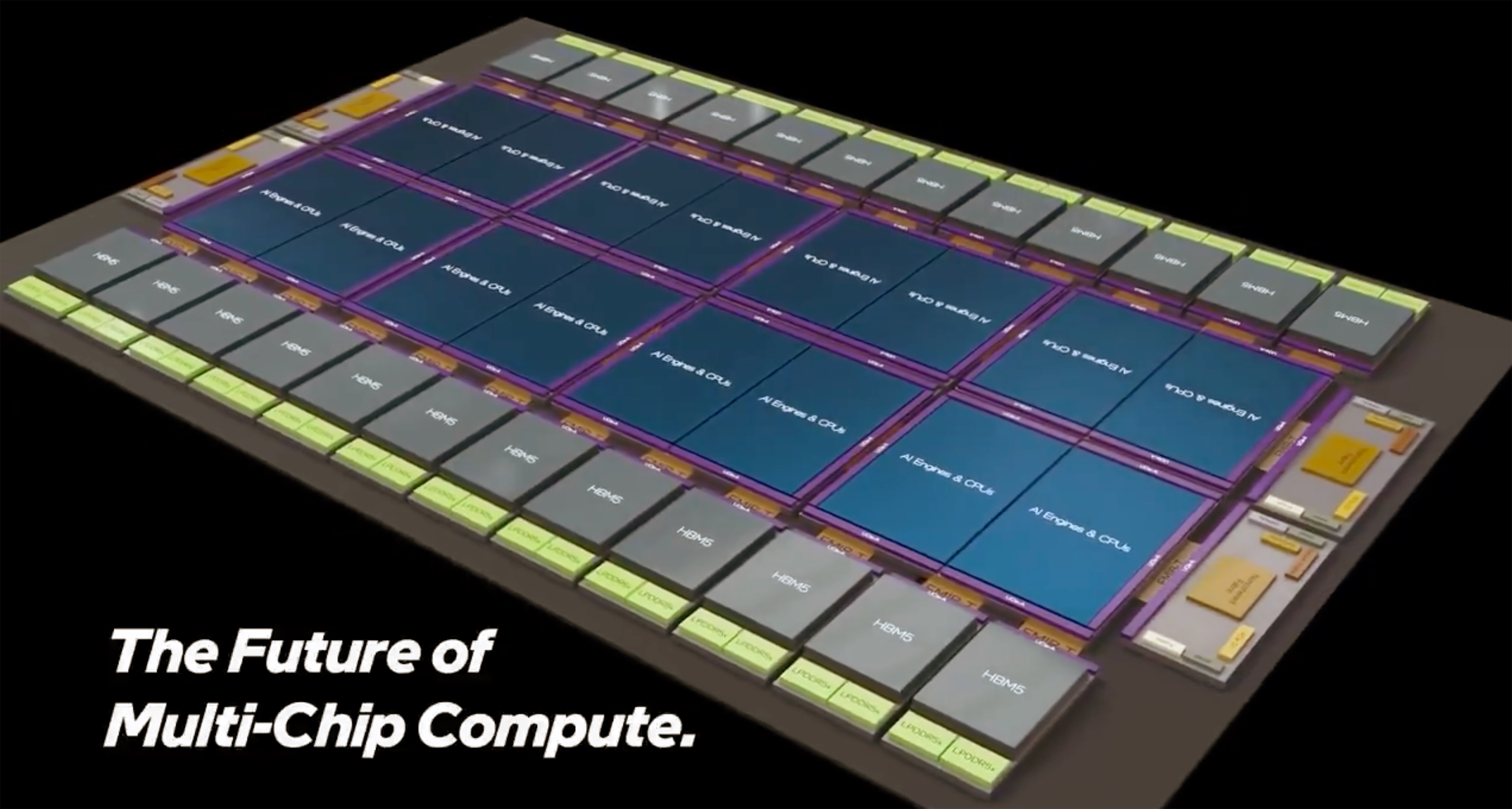
Intel was the first company to build an explicitly disaggregated chiplet design, comprising 47 chiplets, with its Ponte Vecchio compute GPU for AI and HPC applications. This product still holds the record for the most populous multi-tile design, but Intel Foundry envisions something considerably more extreme: a multi-chiplet package that integrates at least 16 compute elements across eight base dies, 24 HBM5 memory stacks, and scales to 12X the size of the largest AI chips on the market ( 12x reticle size, beating TSMC's 9.5x reticle size). Of course, we can only wonder about the power consumption and cooling requirements for such beastly processors.

Intel's conceptual 2.5D/3D multi-chiplet package demonstrates 16 large compute elements (AI engines or CPUs) produced on Intel's 14A or even more sophisticated 14A-E process technology (1.4nm-class, enhanced features, second-gen RibbonFET 2 gate-all-around transistors, improved PowerVia Direct backside power delivery).
These sit on top of eight (presumably reticle-sized) compute base dies made on 18A-PT (1.8nm-class, performance enhanced with through-silicon vias (TSVs), and backside power delivery) that can either do some additional compute work, or pack plenty of SRAM cache for the 'main' compute dies, as Intel shows in its example.
From cutting-edge interconnects to system-level assembly and test, Intel Foundry delivers the scale and integration needed to power next-generation multichip platforms. Https://t.co/smSje92QQh #IntelFoundry #Semiconductors pic.twitter.com/4sAVftVRhg December 22, 2025
*Expand the tweet above to watch the fly-through video.
The base dies are connected to the compute tiles using Foveros Direct 3D, leveraging ultra-high-density sub-10 µm copper-to-copper hybrid bonding to deliver maximum bandwidth and power to the top dies. Intel's Foveros Direct 3D is currently the pinnacle of Intel Foundry's packaging innovations, underscoring the very sophisticated design.
The base dies leverage EMIB-T (an enhanced version of Embedded Multi-Die Interconnect Bridge with TSVs), with UCIe-A on top, for lateral (2.5D) interconnections among themselves and with I/O dies made on 18A-P (1.8nm-class, performance-enhanced), and custom base dies, for up to 24 HBM5 memory stacks.
It is noteworthy that Intel proposes to use EMIB-T with the UCIe-A on top to connect customized HBM5 modules rather than use JEDEC-standard HBM5 stacks with an industry-standard interface, possibly to get more performance and capacity. Given the concept nature of the demonstration, the use of custom HBM5 stacks is not a design requirement; it is simply a way to show that Intel integrates such devices as well.
The whole package can also carry PCIe 7.0, optical engines, noncoherent fabrics, 224G SerDes, proprietary accelerators for things like security, and even LPDDR5X memory for added DRAM capacity.
Get 3DTested's best news and in-depth reviews, straight to your inbox.

Note that the video Intel Foundry posted on X shows two conceptual designs: a 'mid-scale' one featuring four compute tiles and 12 HBM, and an 'extreme' one with 16 tiles and 24 HBM5 stacks, which our story focuses on. Even the mid-scale design is fairly advanced by today's standards, but Intel can produce it today.
As for the extreme concept, this may emerge toward the end of the decade, when Intel has perfected not only Foveros Direct 3D packaging technology but also its 18A and 14A production nodes. Being able to produce such extreme packages towards the end of the decade will put Intel on par with TSMC, which plans something similar and even expects at least some customers to use its wafer-size integration offerings in circa 2027 – 2028.
Making the extreme design a reality in just a few years is a significant challenge for Intel, as it must ensure the components do not warp when attached to motherboards and do not deform even with minimal tolerances due to overheating after prolonged use. Beyond that, Intel (and the whole industry) will need to learn how to feed and cool monstrous processor designs the size of a smartphone (up to 10,296 mm^2) that will have an even larger package, but that's a different story.

Follow 3DTested on Google News, or add us as a preferred source, to get our latest news, analysis, & reviews in your feeds.

-
TechieTwo Intel is just trolling for customers when they can't even get their act together on their own CPUs.Reply -
TerryLaze Reply
This is about (AI) GPUs....TechieTwo said:when they can't even get their act together on their own CPUs.
CPUs,and your opinion on them, are completely irrelevant to this article.
Go ahead and write a few paragraphs on how terrible the GPUs are, maybe that will convince multi billion international companies to not choose intel fabs.......
Intel was the first company to build an explicitly disaggregated chiplet design, comprising 47 chiplets, with its Ponte Vecchio compute GPU for AI and HPC applications. This product still holds the record for the most populous multi-tile design,
-
bit_user Reply
This. Yield and defect management are going to be key, for something like this. I think you basically have to anticipate and handle some of the dies (or their joints) failing, in the field. Otherwise, the field failure rate will likely be way too high.The article said:Making the extreme design a reality in just a few years is a significant challenge for Intel, as it must ensure the components do not warp when attached to motherboards and do not deform even with minimal tolerances due to overheating after prolonged use. Beyond that, Intel (and the whole industry) will need to learn how to feed and cool monstrous processor designs the size of a smartphone -
bit_user Reply
Ponte Vecchio was so late that Intel had to pay a penalty for it delaying the big supercomputer that was its marquee design win.TerryLaze said:Go ahead and write a few paragraphs on how terrible the GPUs are, maybe that will convince multi billion international companies to not choose intel fabs.......
Intel was the first company to build an explicitly disaggregated chiplet design, comprising 47 chiplets, with its Ponte Vecchio compute GPU for AI and HPC applications. This product still holds the record for the most populous multi-tile design,
Worse, it reportedly had yields of less than 10%, which goes to one of my points in the prior post. Granted, that's because they had no ability to test the individual chiplets before assembly. But, the unit highlighted in the article has way more complexity, is made on even smaller nodes, and will likely be pushed way harder than Ponte Vecchio ever was. So, field failures of individual chips & stacks are going to be a live issue, in products of this sort. -
thestryker Reply
I don't think it'd be crazy to say that Intel learned more about packaging from Ponte Vecchio than everything else they've done. There haven't been any reports regarding failure rates so I doubt there's anything beyond standard expectations. I don't believe they ended up clocking them as high as planned though which is likely due to improving long term reliability.bit_user said:Ponte Vecchio was so late that Intel had to pay a penalty for it delaying the big supercomputer that was its marquee design win.
Worse, it reportedly had yields of less than 10%, which goes to one of my points in the prior post. Granted, that's because they had no ability to test the individual chiplets before assembly. But, the unit highlighted in the article has way more complexity, is made on even smaller nodes, and will likely be pushed way harder than Ponte Vecchio ever was. So, field failures of individual chips & stacks are going to be a live issue, in products of this sort.
From what we've seen so far with interconnected chips the interconnects themselves don't seem to be a failure point. Of course the chips being much larger does mean there's just flat out more to fail. I'd like to think that anyone leveraging these huge interconnected designs would build in a way to keep operating in a degraded state whenever possible to mitigate failures. -
bit_user Reply
I think the launch problems with Blackwell B200 are a good reminder of the sorts of things that can happen with advanced packaging and large dies:thestryker said:From what we've seen so far with interconnected chips the interconnects themselves don't seem to be a failure point. Of course the chips being much larger does mean there's just flat out more to fail.
"Nvidia's Blackwell B100 and B200 GPUs link their two chiplets using TSMC's CoWoS-L packaging technology, which relies on an RDL interposer equipped with local silicon interconnect (LSI) bridges (to enable data transfer rates of about 10 TB/s). The placement of these bridges is critical. However, a supposed mismatch in the thermal expansion properties between the GPU chiplets, LSI bridges, RDL interposer, and motherboard substrate caused the system to warp and fail, and Nvidia reportedly had to modify the top metal layers and bumps of the GPU silicon to enhance production yields."
Source: https://www.3dtested.com/tech-industry/artificial-intelligence/nvidias-jensen-huang-admits-ai-chip-design-flaw-was-100-percent-nvidias-fault-tsmc-not-to-blame-now-fixed-blackwell-chips-are-in-production -
thestryker Reply
Yeah I wondered if this was a cost of pushing to get hardware out so quickly. It was a problem that really should have been caught during a normal QA cycle.bit_user said:I think the launch problems with Blackwell B200 are a good reminder of the sorts of things that can happen with advanced packaging and large dies -
bit_user Reply
That was caught before they did the volume ramp. It was the reason for the launch being delayed, I think because you don't expect to have such major problems arising and it took more time to address than the typical issues you'd fix with something like a metal layer change.thestryker said:Yeah I wondered if this was a cost of pushing to get hardware out so quickly. It was a problem that really should have been caught during a normal QA cycle. -
TerryLaze Reply
Hey, you did it!bit_user said:Ponte Vecchio was so late that Intel had to pay a penalty for it delaying the big supercomputer that was its marquee design win.
Worse, it reportedly had yields of less than 10%, which goes to one of my points in the prior post. Granted, that's because they had no ability to test the individual chiplets before assembly. But, the unit highlighted in the article has way more complexity, is made on even smaller nodes, and will likely be pushed way harder than Ponte Vecchio ever was. So, field failures of individual chips & stacks are going to be a live issue, in products of this sort.
With so much undisputable evidence potential customers aren't going to do any actual wafer yield tests on the actual node with any actual designs and will instead just not use intel...Great job!
