Microsoft-backed start-up raises $40 million for helium atom beam lithography that could print chips at atomic resolution — 0.1nm beam is 135 times narrower than ASML's EUV light
Stay On the Cutting Edge: Get the 3DTested Newsletter
Get 3DTested's best news and in-depth reviews, straight to your inbox.
You are now subscribed
Your newsletter sign-up was successful
An account already exists for this email address, please log in.
Subscribe to our newsletter
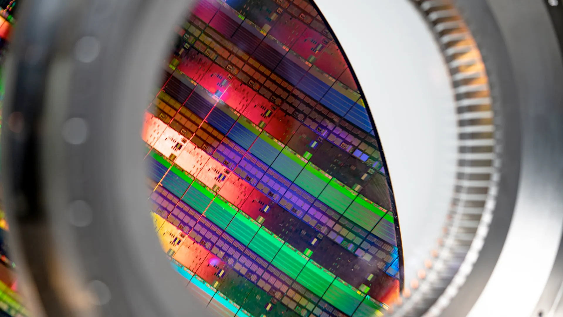
Lace Lithography, a Norwegian start-up backed by Microsoft, raised $40 million in Series A funding on Monday to develop a chipmaking tool that uses a helium atom beam instead of light to pattern silicon wafers, Reuters reported. The company claims its technology can create chip features 10 times smaller than current lithography systems, with a beam width of just 0.1 nanometers compared to the 13.5nm wavelength used by ASML's EUV scanners. Lace aims to have a test tool running in a pilot fab by 2029.
The advantage of Lace’s system is that atoms don’t have a diffraction limit, whereas photon-based lithography, including ASML's EUV systems, is constrained by the wavelength of the light it uses. As chipmakers push features smaller, they rely on increasingly complex multi-patterning techniques to work around that limit, but Lace sidesteps the problem entirely by replacing photons with neutral helium atoms and a beam measuring roughly the width of a single hydrogen atom.
John Petersen, scientific director of lithography at Imec, told Reuters that the approach could shrink transistors and other features by an order of magnitude to an "almost unimaginable" degree. Bodil Holst, CEO and co-founder of Lace, said the technology would enable chip manufacturers to print wafers at "ultimately atomic resolution."
Article continues below
Lace describes its systems as "BEUV," or Beyond-EUV. The company was founded in 2023 by Holst, a physicist affiliated with the University of Bergen, and co-founder Adrià Salvador Palau. It now employs more than 50 people across Norway, Spain, the UK, and the Netherlands, and presented its findings at the SPIE Advanced Lithography + Patterning 2026 conference last month.
Lace joins a growing roster of start-ups developing alternatives to ASML's near-monopoly on advanced lithography. U.S.-based Substrate and xLight are both building particle accelerator-driven light sources for EUV or X-ray lithography, with xLight receiving $150 million in U.S. Government funding. Canon shipped its first nanoimprint lithography tool to the Texas Institute for Electronics back in September 2024, and China's Prinano has delivered its own nanoimprint system domestically.
Lace's approach, however, differs from all of these. Where Substrate and xLight still rely on photons, Lace abandons electromagnetic radiation altogether, meaning that its approach has no existing ecosystem of process flows to plug into.
While Lace has built prototype systems, the gap between the lab and production is, as always, huge. The company is currently targeting 2029 for the deployment of a test tool in a pilot facility, with any eventual move to volume manufacturing unlikely to follow for a long time after that. ASML spent decades and billions of dollars turning EUV from a research concept into a commercial product, and even well-funded newcomers face a long road to viability.
Stay On the Cutting Edge: Get the 3DTested Newsletter
Get 3DTested's best news and in-depth reviews, straight to your inbox.