
UALink roadmap plots course to optimized AI data center interconnects — examining the open standard designed to combat vendor lock-in while offering cost and performance optimization

UALink (short for Ultra Accelerator Link) is an upcoming interconnect technology designed to enable high-speed, low-latency communication between AI accelerators (ASICs, GPUs, FPGAs, NPUs, XPUs) and other compute devices across a scale-up logical domain. Many see it as an important path forward for the future of AI data centers due to its planned performance, cost, and power efficiency advantages, not to mention that, as an open standard, it will reduce vendor lock-in.
In 2025, the UALink Consortium published revision 1.0 of the UALink specification, marking a point after which hardware designers can officially implement the technology into their AI/HPC accelerators and switch ASICs required to build AI pods with up to 1,024 accelerators. But while UALink technology is widely supported by the industry, and its specification that defines accelerator-to-accelerator comms is available now, its broad adoption is several years away.
What is UALink?
UALink would enable programmers to treat multiple accelerators like a single processor, with a large memory pool (or at least enable parallelism with minimal effort from developers) and to greatly simplify network communications between processors.
UALink was designed as a competing technology for Nvidia's proprietary NVLink interconnect that is supported by a broad range of industry players, including AMD, Arm, AWS, Broadcom, Cadence, Intel, Google, Marvell, Meta, Microsoft, and Synosys, just to name a few.
The UALink 200G 1.0 specification is designed to support up to 1,024 accelerators per domain (or pod) at a speed of 212.5 GT/s, enabling direct memory access between accelerators using simple load/store and atomic operations, and thus behaves as a single system. UALink is built around a lightweight layered protocol stack that includes a Protocol Layer (UPLI), Transaction Layer (TL), Data Link Layer (DL), and Physical Layer (PL).

At the physical layer, UALink reuses standard Ethernet PHY signaling (such as 100GBASE-KR1, 200GBASE-KR2, and 800GBASE-KR4) to simplify implementation, but introduces custom framing, forward error correction (FEC), and latency optimizations. Each serial lane runs at 212.5 GT/s, delivering an effective 200 GT/s of data per lane after FEC overhead. Meanwhile, configurations of x1, x2, or x4 links are supported, to enable up to 800 GT/s of bandwidth per direction per link. The DL layer formats traffic into 640-byte FLITs with CRC and segment headers, while the TL layer compresses request and response messages into 4–16 byte payloads to cut latencies and keep die area in check.
According to developers of UALink, the protocol ensures deterministic latency below 1 µs and achieves up to 93% effective bandwidth utilization, which is very high. UALink does not replace Ethernet, PCIe, or CXL, but is designed to coexist with these technologies within system nodes, serving solely for peer-to-peer traffic between accelerators.
When it comes to system architecture, it is centered around UALink Switches (ULS) that enable point-to-point accelerator communication within and across racks. These switches must support lossless delivery, non-blocking fabric behavior, and virtual pod isolation. Each accelerator is assigned a 10-bit routing ID (thus the limitation of 1,024 accelerators per pod), and switches maintain per-port routing tables to support scale-up topologies. The standard includes fault containment, error detection, and isolation mechanisms that limit failures to a single virtual pod without impacting others in the 'large' scale-up pod.
While UALink version 1.0 is here, the technology is still a work in progress as future versions are expected to add memory coherency (already supported by NVLink) and virtualization features.
Why UALink?

Today, Nvidia's NVLink allows the company and its partners to build pods with up to 576 GPUs (GPU packages), enabling scale-up world sizes that feature both high bandwidth and low latency. In contrast, the scale-up world size of AMD's Instinct MI300-series accelerators (or Nvidia's H100 GPUs) is limited to eight GPUs per box, as connectivity outside of the box is enabled by Ethernet.
Ethernet, even at 400G/800G with RDMA (RoCE), is fundamentally optimized for packet-based, scale-out communication, not the low-latency, memory-semantic, load/store operations required for scale-up AI accelerator interconnects. By contrast, UALink provides direct memory access between accelerators, supports atomics, and preserves ordering semantics across endpoints. Even with various optimizations, Ethernet introduces higher round-trip latency (~2 µs+) and software stack overhead, something that limits Ethernet even for modern data centers. By contrast, UALink targets <1 µs round-trip latency, supports lossless flow control, and operates with fixed-size FLITs and ID-based routing.
Even high-end Ethernet switches like Broadcom's Tomahawk Ultra require NICs to translate load/store commands into RDMA commands, which adds latency and complexity that UALink bypasses by supporting native hardware messaging.
Building the UALink ecosystem
As the UALink Consortium includes over 90 members, it is reasonable to assume that there are dozens of companies currently working on various AI and HPC accelerators with UALink support. In addition, connectivity companies are working on switches. Finally, Synopsys has been offering UALink IP and PHY for about a year now, which greatly simplifies the implementation of the technology.
Integrating ready IP and PHY from vendors like Synopsys or Cadence into an AI accelerator or system-on-chip typically takes 12 to 24 months, depending on the complexity of the chip, project maturity, and some other development-specific factors. Therefore, processors with UALink could be months or quarters away. Synopsys says that the interest in the technology is significant.
"UALink is a truly open standard that is attracting significant interest from both accelerator and switch companies," Priyank Shukla, Director of Product Management for HPC IP at Synopsys, told 3DTested. "We have successfully delivered our Synopsys UALink 200G IP solution, which includes both controller and PHY IP, to customers in the switch and accelerator markets."
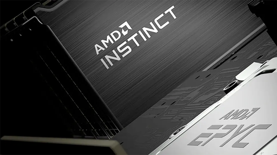
Among the companies that have already confirmed development of processors with UALink are AMD (Instinct MI400, MI500-series) and Marvell (as an option for custom silicon aimed at hyperscalers), though expect the technology to be supported by others shortly. However, the deployment of UALink switches across the MI400 series is dependent on how quickly we can see UALink switching silicon in 2026. In the absence of such switches, the MI400 series may be forced to use UALink-over-Ethernet, which is a less-than-ideal use case.

In fact, it looks like the availability of switches could be the main factor that slows down the adoption of UALink technology.
Astera Labs is currently developing smart fabric switches, signal conditioners, controllers, and more. The company expects to deliver its first UALink solutions in 2026 to solve scale-up connectivity challenges, but it has not disclosed what comes next. It also observes that the interest in the technology is significant.
"While I cannot speak to specific product timelines, what I can tell you is that the UALink ecosystem momentum has exceeded our expectations since releasing the 1.0 specification in April," Chris Petersen, Fellow of Technology and Solution Architecture at Astera Labs, told 3DTested. "Our customers — particularly hyperscalers — consistently tell us three things drive their infrastructure decisions: they need open standards with multi-vendor support, they're focused on total cost of ownership, and they need faster time-to-market to deploy the compute scale that cutting-edge AI applications demand."
Unlike Astera Labs, Broadcom — which develops custom AI processors for its clients as well as various communications hardware for data centers — seems a little more restrained, even though it is a founding member of the UALink Promoters Group. The company cannot talk about whether it is building UALink-supporting accelerators for its customers, and it positions its Tomahawk Ultra Ethernet solutions for scale-up connectivity of AI accelerators.
"We can say that we see tremendous momentum behind using Ethernet for scale-up," a spokesperson for Broadcom told us. "Tomahawk Ultra was purpose-built for Ethernet-based AI scale-up and is available today."
Is there a roadblock?
Although the UALink 1.0 specification is ready and can be used to build switching hardware, the technology is missing several things, including the 128G DL/PL specification (was expected in July 2025, but there is no word whether it has been finalized), In-Network Collectives (INC, was expected December 2025) hardware acceleration of collective operations, and a 128G/200G UCIe PHY chiplet specification.
None of these features is mandatory for building switching hardware, so building a spec-compliant switch ASIC under the UALink 1.0 is possible. However, the 128G DL/PL specification will be important for next-gen, mixed-rate, or forward-compatible switch designs that support a slower data transfer rate. Meanwhile, INC is required to support large-scale training efficiently and interoperate with future hardware. Without INC, collective operations must be executed in software or via network cards, which adds latency and hinders the advantages of UALink.
"The UALink Consortium is actively working on additional specifications,s including management, UCIe IO chiplet integration, and In-Network Collectives that will further enhance the ecosystem to meet these demands," said Petersen. "With 85+ member companies driving this expanding specification roadmap, UALink is responding to a real market urgency for scale-up solutions that can keep pace with AI's exponential growth."
Perhaps some of the companies that currently work on UALink-supporting hardware do not want to commit to a particular roadmap before all the features are supported by the specification. However, the importance of INC may not be that significant.
"INC is not commonly deployed across all applications, and we also see many of today's solutions that could use INC are deployed without INC enabled," Ahmad Danesh, Associate Vice President of product management at Astera Labs, told 3DTested. "The UALink Consortium BoD considered this when defining UALink 1.0, and the early adopters see a higher priority on delivering higher performance and lower TCO through UALink's purpose-built memory-semantic protocol. The lack of INC specification in UALink 1.0 is not expected to affect launch schedules of UALink hardware, but the consortium continues to advance the specification and actively works on INC to deliver even more value with UALink."
Adoption will take time
UALink is a promising and open interconnect standard designed to enable high-speed, low-latency communication between AI accelerators that has gained support from over 90 companies.
However, while AMD and Marvell have confirmed UALink-based processor development and Synopsys already offers controller and PHY IP, full-scale deployment will take time due to integration cycles and the current lack of UALink-compliant switches.
Although future enhancements like In-Network Collectives (INC) and the 128G PHY spec are not required to build compliant hardware, their absence may delay broader commitments, as some companies may wait for these features to be finalized before locking development of their UALink hardware and releasing it to market. Nonetheless, Astera Labs expects the first products supporting UALink to hit the market at some point this year.
