Razer laptop motherboard repair video showcases superhuman hand-soldering skills — PCB damage appears to be the result of a misplaced screw hole on a motherboard that one repairer says has 'a fatal design flaw'
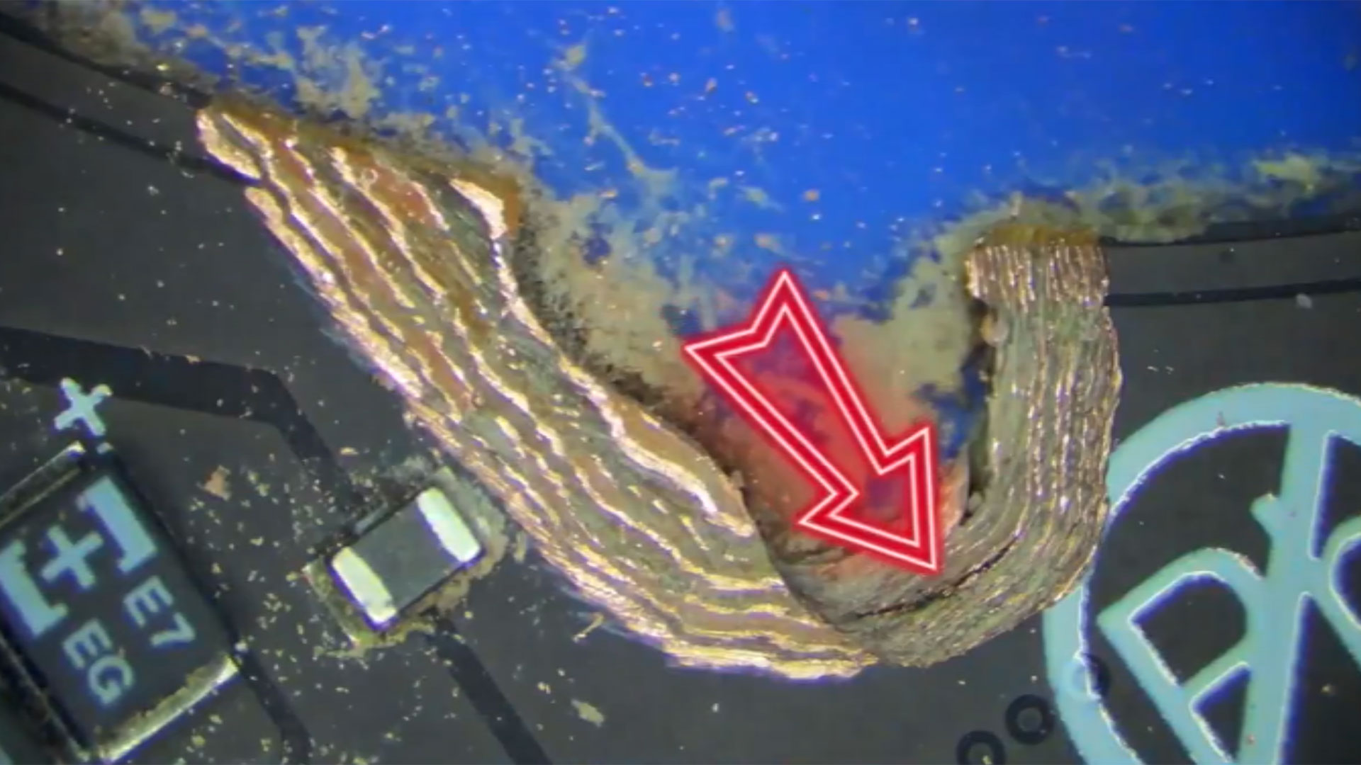
Tiny trace repair work needed to be replicated across several PCB layers.
Get 3DTested's best news and in-depth reviews, straight to your inbox.
You are now subscribed
Your newsletter sign-up was successful
An electronics technician stars in a video showing an intricate repair of a Razer gaming laptop motherboard by hand. This is one of the most challenging PCB repair tasks we have seen come to a successful conclusion. The repair fixes damage that appears to be the result of the same underlying issue outlined by another repair tech, who asserts that Razer’s Blade 14 mobo has “a fatal design flaw.”
It is definitely worth spending two minutes and 48 seconds watching this, even if you watch it at 2x speed, but you then need to remember to pick up your jaw from the floor.
Repairing a Razer motherboard damaged by a screw. Pic.twitter.com/HwPEdcL2D7 December 26, 2025
Being adept at electronics repair is an enviable skill. Moreover, as components are continuously miniaturized, such highly skilled work pushes the bounds of human-level ability. In the above video, we see an unnamed technician work on a severely damaged Razer laptop motherboard.
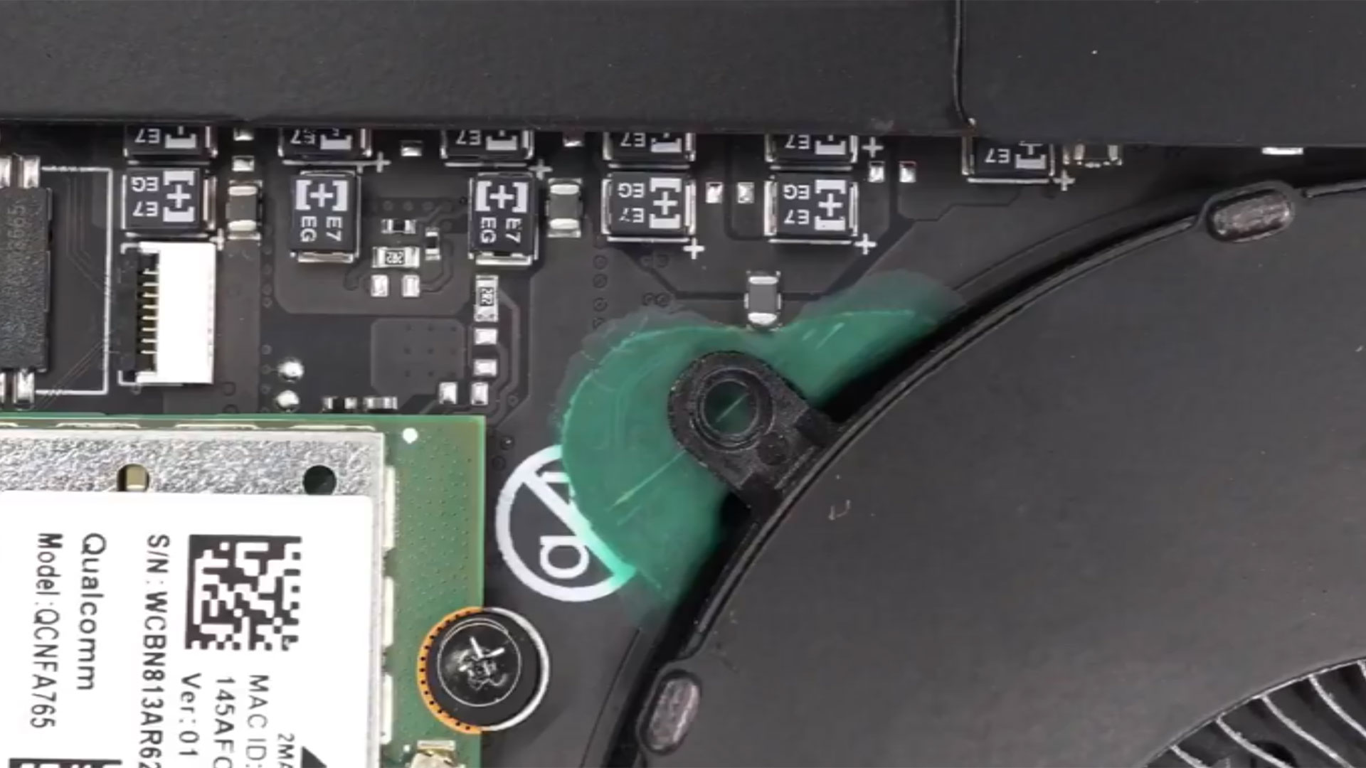
Article continues belowThe video begins with a close-up of the laptop motherboard, showing a chunk of its structure around a screw hole that is obviously missing. We'll discuss the potential causes of this damage later...
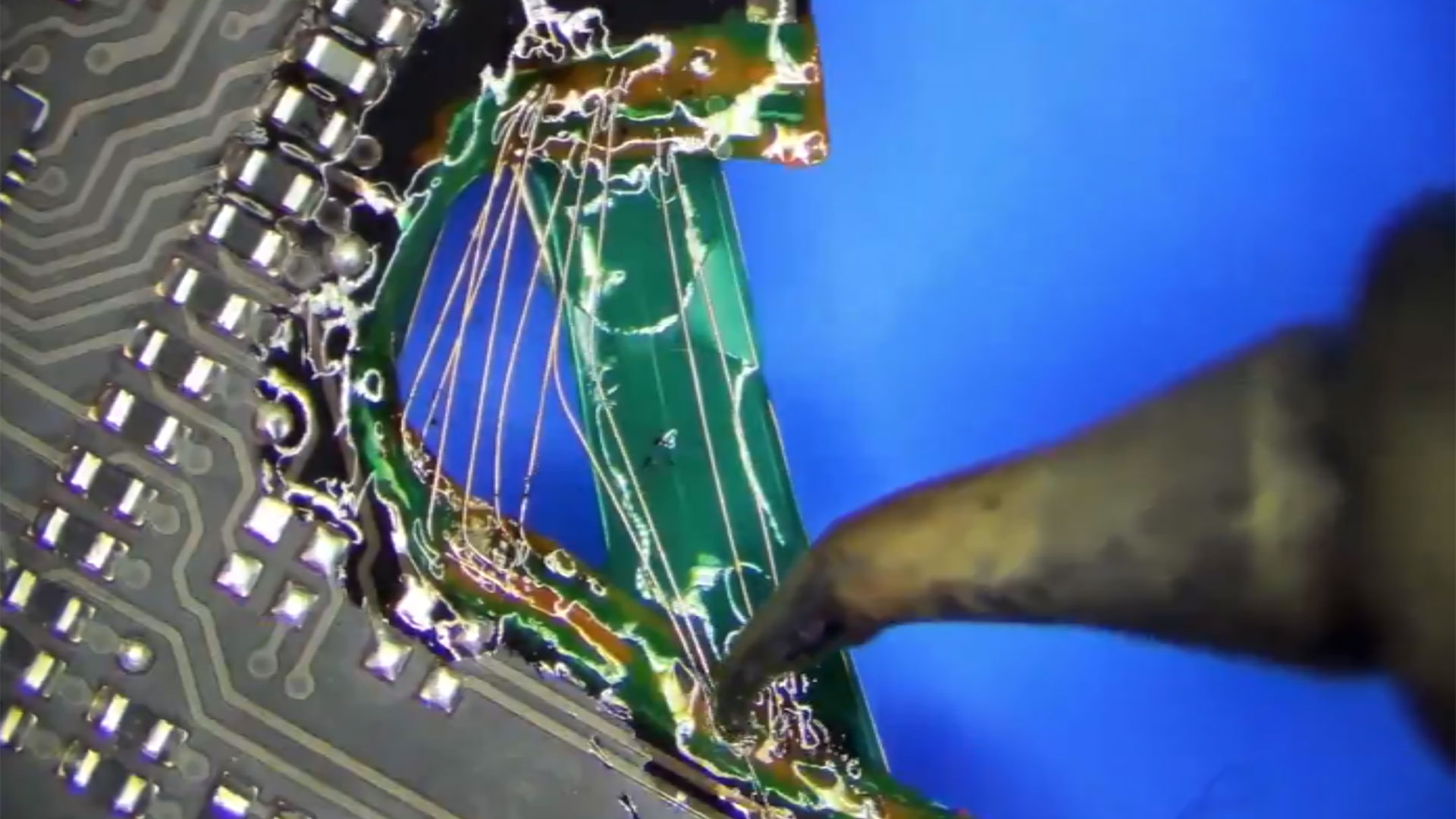
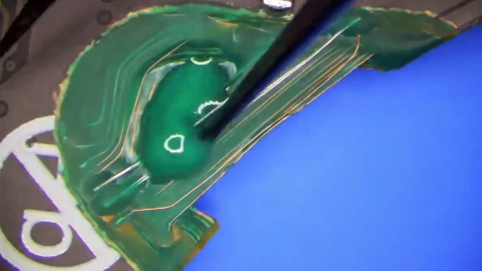
As a first step, the technician uses a grinding pen and takes away material at an angle. This work provides improved access to the multiple conductive layers of the PCB, enabling them to be addressed separately during upcoming soldering repairs. Think of this task a little like how ancient rice farmers would terrace the side of a mountain to provide workable paddy fields.
Pausing the video, we can see the deft grinding pen work makes more than 10 PCB layers distinguishable. Once they are happy with the layer exposure, the technician moves to the intricate cleaning of circuit traces at the chosen level to prepare them for reconnecting using hair-thin enameled wiring.
The technician deftly solders the first target PCB layer with their iron and ultra-thin connecting wires. With the first of several layers now considered fixed, solder mask is applied to insulate and add structure where it is currently missing. This meticulous work was repeated across several layers, restoring the damaged PCB both electrically and structurally.
Get 3DTested's best news and in-depth reviews, straight to your inbox.
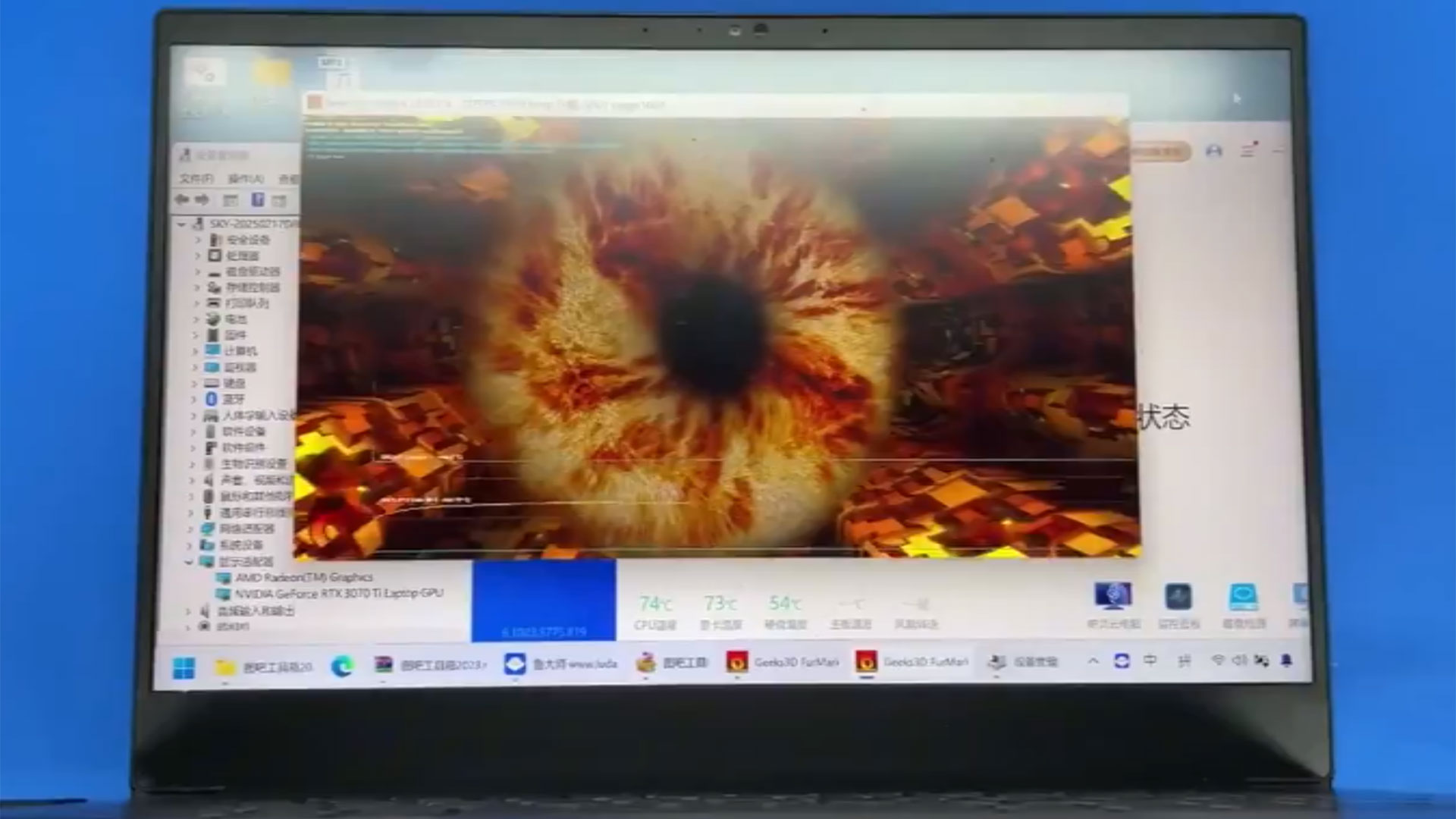
Finally, the job is complete: the laptop cooling assembly is reattached, and the machine is reassembled. As ‘proof’ of a successful job, the video ends with a brief clip of the purported same laptop running FurMark – the (in)famously punishing benchmark and PC stress test. At this stage, we see Simplified Chinese text in the Windows UI, hinting that this repair was done in China.
Is this Razer laptop design prone to cooler screw-induced damage?
This particular issue with the Razer Blade seems to be more common than it should be. There is a screw hole in the PCB near one of the cooling fans. Our research indicates that this particular hole is a little bit too close to a high-power voltage trace. Thus, maintenance, where this screw is removed/inserted, can cause electrical arcing and result in difficult-to-repair damage. This video covers what seems to be the same underlying issue, and asserts that Razer’s Blade 14 mobo has “a fatal design flaw.”

Follow 3DTested on Google News, or add us as a preferred source, to get our latest news, analysis, & reviews in your feeds.

-
Co BIY ReplyFruitmaniac said:How do they know which leads to connect??? 😭
Agree. The success of this repair depends on it being a pretty simple part of the board. Where new contact to new contact could be figured out in simple left to right order.
Amazing work. -
bit_user Reply
I think they must've gotten a schematic from the manufacturer.Fruitmaniac said:How do they know which leads to connect??? 😭
With a simpler board, if you have a known good example, perhaps you could try using a meter to test connectivity, but I don't know if that's even feasible with such complex, multi-layered PCBs as this.
The typical repair for such damage would be just to find a used laptop of the same model and transplant its motherboard. It'd probably need to have the same (or better) CPU as well, since that's soldered down. Yeah, you could transplant CPU/GPU to a different board, but that's even more labor intensive than this rework. -
helper800 Reply
In my opinion, transplanting a CPU from one board to another is way less work than what this guy did to fix those traces and reform the PCB.bit_user said:I think they must've gotten a schematic from the manufacturer.
With a simpler board, if you have a known good example, perhaps you could try using a meter to test connectivity, but I don't know if that's even feasible with such complex, multi-layered PCBs as this.
The typical repair for such damage would be just to find a used laptop of the same model and transplant its motherboard. It'd probably need to have the same (or better) CPU as well, since that's soldered down. Yeah, you could transplant CPU/GPU to a different board, but that's even more labor intensive than this rework. -
bit_user Reply
How many hours do you think each takes? It can be hard to get a sense of the real time involved, when watching youtube videos.helper800 said:In my opinion, transplanting a CPU from one board to another is way less work than what this guy did to fix those traces and reform the PCB.
From watching GPU repairs, I think removing two CPU, then cleaning one CPU + board and reballing a CPU with ~2000 pads is very time-consuming. As delicate as this motherboard repair was, the actual number of wires was far lower. Yeah, they had to build up PCB layers as they went, but I still think it'd be less time. -
alan.campbell99 Better than my average solder skills certainly. Best I can do with a solder station iron is a one off project where I had to change several SMD resistors on some Dell laptop mainboards, think they were 1mm or so. Damned fiddly it was for me. Old boss at a previous work was better at that. I wouldn't even try removing and reballing.Reply -
JohnyFin Again klick bytes project for public. It can be possible, it is possible but is not practical at all. Is just next weird Mount Everest. Probably next pseudo project will be reap off in half whole motherboard and rapir it. This projects proofs nothing and it has no sense.Reply -
rcx The easiest way to do this would be with board layer information, which no manufacturer is going to supply. Schematics alone would be extremely difficult. You would have to find the source and destination(s), by trial and error. Then there are things like guard traces for some signals, blind vias, etc. I am impressed enough that someone could solder those wires in place as straight as they did, not touching. I think it is a great soldering job, but it is otherwise not real.Reply

